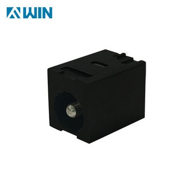
What Is The Function Of The Wafer Connector Terminal in The PCB Board
May 15, 2024
The wafer connector terminal serves as a critical component in facilitating electrical connections on a printed circuit board (PCB). Its primary function is to establish a reliable and secure interface between the PCB and external components, wires, or other PCBs within an electronic system. Here's an in-depth exploration of the function and significance of wafer connector terminals on a PCB:
Interconnection: At its core, the wafer connector terminal enables the interconnection of various electronic components, modules, or subsystems on the PCB. It acts as the intermediary point where signals, power, or data are transmitted between different parts of the circuit or between multiple PCBs within the system.
Signal Transmission: One of the fundamental functions of wafer connector terminals is to transmit electrical signals between different elements of the circuit. Whether carrying analog signals, digital signals, or control signals, the terminals ensure efficient and reliable signal transmission without distortion or loss.
Power Distribution: In addition to transmitting signals, wafer connector terminals also facilitate the distribution of power across the PCB. They serve as pathways for delivering voltage and current to various components or subsystems, ensuring stable and consistent power supply throughout the system.
Mechanical Support: Beyond their electrical role, wafer connector terminals provide mechanical support and anchoring for the connected components or wires. By securely holding the inserted connectors or wires in place, they prevent accidental disconnection or movement due to vibration, shock, or external forces.
Flexibility and Modularity: Wafer connector terminals contribute to the flexibility and modularity of PCB design. They enable easy customization and reconfiguration of electronic systems by providing a standardized and versatile connection interface. Designers can readily swap or upgrade components without the need for extensive redesign of the PCB layout.
Space Optimization: Wafer connector terminals play a crucial role in space optimization on the PCB. Their compact and low-profile design allows for high-density packaging of components, minimizing the overall size and footprint of the electronic system. This is particularly beneficial in applications where space is limited or where miniaturization is desired.
Reliability and Durability: Wafer connector terminals are engineered for reliability and durability, ensuring long-term performance in demanding operating conditions. They are constructed from high-quality materials, such as metals or high-temperature plastics, and undergo rigorous testing to withstand temperature extremes, vibration, moisture, and other environmental factors.
Ease of Assembly and Maintenance: Finally, wafer connector terminals contribute to the ease of assembly and maintenance of electronic systems. They support various termination methods, including surface mount, through-hole, and crimping, making them compatible with different assembly techniques and equipment. This simplifies the manufacturing process and facilitates troubleshooting and repair tasks during the system's lifecycle.
In summary, the wafer connector terminal serves multiple functions on a PCB, including interconnection, signal transmission, power distribution, mechanical support, flexibility, space optimization, reliability, and ease of assembly. Its versatility and importance make it an indispensable component in modern electronic systems across various industries and applications.